Lathrop had actually invested years checking out microscopic lens to make something little appearance larger. As he puzzled over how to miniaturize transistors, he and Nall questioned whether microscopic lense optics turned upside down might let something huge– a pattern for a transistor– be miniaturized. To learn, they covered a piece of germanium product with a kind of chemical called a photoresist, which they obtained from Eastman Kodak, the video camera business. Light responds with photoresist, making it either harder or weaker. Lathrop benefited from this function and produced a “mask” in the shape of a mesa, putting it on the microscopic lense with upside-down optics. Light that travelled through holes in the mask was diminished by the microscopic lense’s lens and forecasted onto the photoresist chemicals. Where the light struck, the chemicals solidified. Where light was obstructed by the mask, they might be gotten rid of, leaving an exact, mini mesa of germanium. A method to produce miniaturized transistors had actually been discovered.
Lathrop called the procedure photolithography– printing with light– and he and Nall declared a patent. They provided a paper on the subject at the yearly International Electron Gadgets Satisfying in 1957, and the Army granted him a $25,000 reward for the creation. Lathrop purchased his household a brand-new station wagon with the cash.
In the middle of the Cold War, the marketplace for mortar fuzes was growing, however Lathrop’s lithography procedure removed due to the fact that business producing transistors for civilian electronic devices understood its transformative capacity. Lithography not just produced transistors with extraordinary accuracy however likewise unlocked to additional miniaturization. The 2 business leading the race to business transistors– Fairchild Semiconductor and Texas Instruments– comprehended the ramifications early on. Lithography was the tool they required to produce transistors by the millions, turning them into a mass-market great.
Painting with light
Robert Noyce, among the cofounders of Fairchild, had actually studied along with Lathrop when both had actually been PhD trainees in physics at MIT. The 2 of them had actually invested their weekends in graduate school treking New Hampshire’s mountains, and they had actually remained in touch after finishing. At Fairchild, Noyce moved rapidly to employ Nall, Lathrop’s laboratory partner, and led his business’s lithography efforts by jury-rigging his own gadget with a set of 20-millimeter video camera lenses he ‘d purchased from a Bay Location photography store.
Lathrop, on the other hand, took a task at Fairchild’s rival, Texas Instruments, driving his brand-new station wagon to Dallas. He showed up simply as his brand-new associate and long-lasting buddy Jack Kilby was on the edge of producing a piece of semiconductor product with several electronic parts developed– or incorporated– into it. These incorporated circuits, it quickly ended up being clear, might be effectively produced just with Lathrop’s lithography approach. As chip companies make every effort to diminish transistors to stuff more of them onto chips, photolithography supplied the accuracy that miniaturized production needed.
Fairchild and Texas Instruments made their very first lithography makers in home, however the growing intricacy of the makers quickly brought in brand-new entrants. As the scale of transistors decreased from centimeters to millimeters to microns, the significance of accuracy optics increased. Perkin-Elmer was a Connecticut-based company that produced specialized optics for the United States military, from bombsights to spy satellites. In the late 1960s, it understood that this competence might be utilized for lithography, too. It established a scanner that might predict the mask pattern onto a silicon wafer while aligning them with nearly perfect accuracy. The scanner then moved a light throughout the wafer like a photocopier, painting it with lines of light. This tool showed efficient in producing transistors as little as a micron– one millionth of a meter.
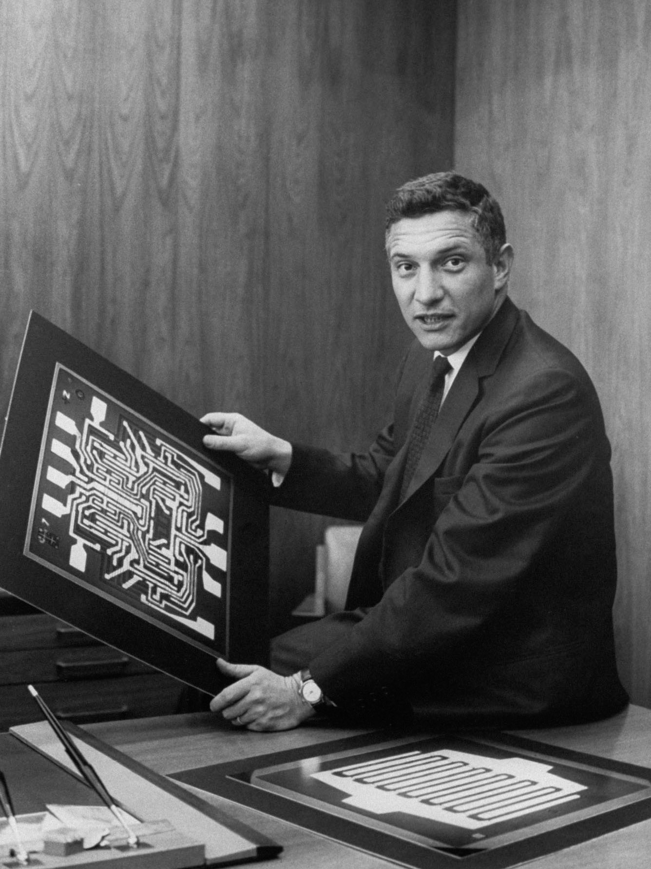
TED STRESHINSKY/GETTY IMAGES
However the method wasn’t useful as chip functions got still smaller sized. By the late 1970s, scanners started to be changed with steppers, makers that moved light in discrete actions throughout a wafer. The obstacle with a stepper was to move the light with micron-scale accuracy, so that each flash was completely lined up with the chip. GCA, a Boston-based company that had its origins in spy balloons, designed the very first stepper tool, apparently on the guidance of Texas Instruments executive Morris Chang– later on the creator of TSMC, which is today the world’s biggest chipmaker.
New England’s expert lithography companies quickly dealt with high competitors. In the 1980s, as Japanese chipmakers started winning significant market share in the production of memory chips, they began purchasing from Nikon and Canon, 2 homegrown manufacturers of lithography tools. Around the exact same time, the Dutch chipmaker Philips drew out its own system that made lithography tools, calling the brand-new business ASML.